Reflection at the Start of the Day
We looked at our day 2 documentation at the start of the day with Mr. Kris and he gave some general feedback:
- Videos should always be recorded in horizontal format to fit neatly into the website layout. Vertical videos take up an excessive amount of vertical space and break the flow of the documentation.
- The project source files (src) are among the most important parts of Fab Academy documentation. These files allow others to reproduce the work, evaluate the design choices, and understand how the electronics and code came together.
Also I also adjusted and made my documentation more detailed for day 2 to start the day. I also listened to my friends’s documentation to understand what they’ve been up to the previous day.
After, Kris showed us a few things:
- 1920x1080 is the default video and photo size for all documentation. It’s basically a horizontal photo taken from a phone camera. USE HORIZONTAL VIDEOS.
- You can use the canvas in Obsidian to create graphics very easily.
- [[Electronic Production Process.canvas|Electronic Production Process]]
Soldering Our Boards
Now we move on to soldering the boards we milled previously. Before starting, Kris explained general soldering fundamentals:
- How to heat both the pad and the component pin evenly
- How to avoid lifting copper pads by keeping the iron on the board for too long
- Why flux is essential even if the solder already contains some. You can never have too much flux!
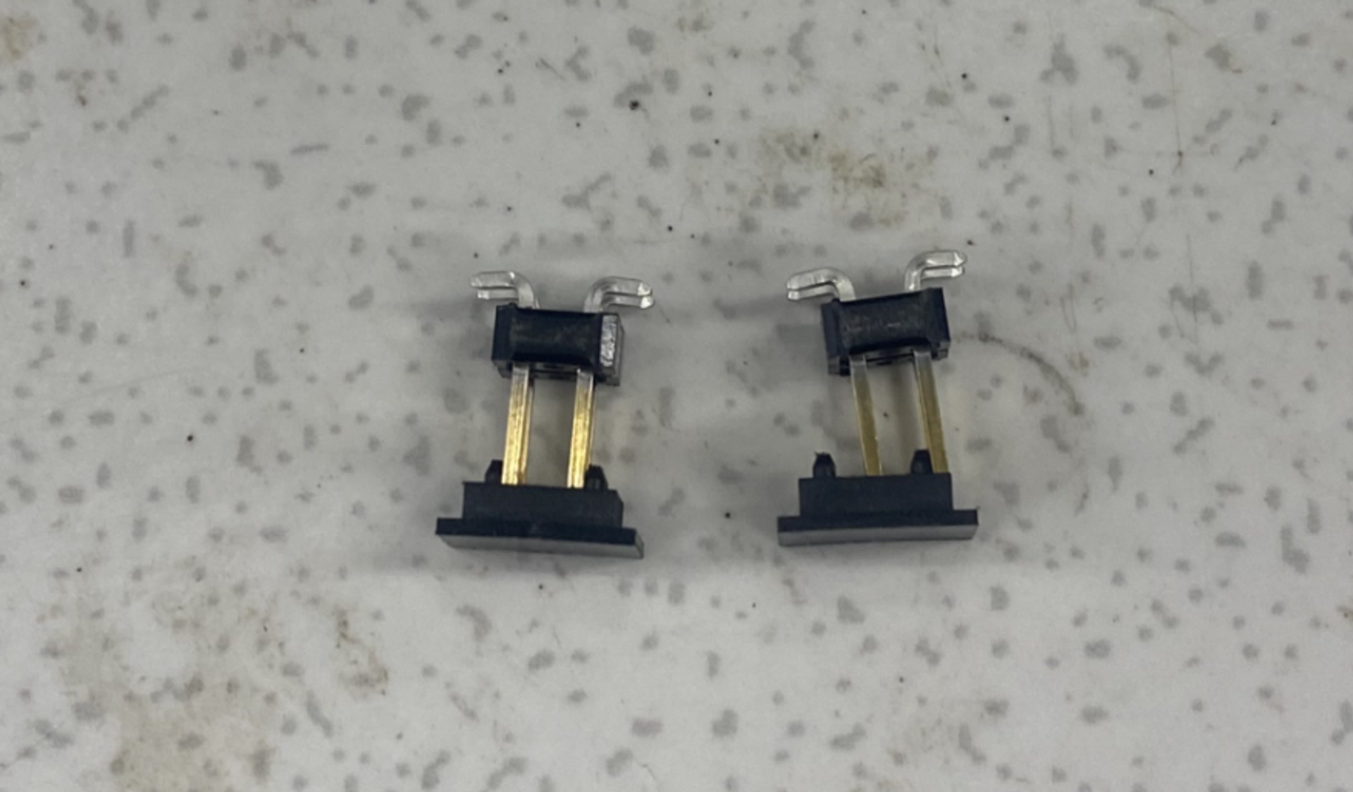
Firstly, I created the cables for the i2c connection between boards. You can see the components used below:
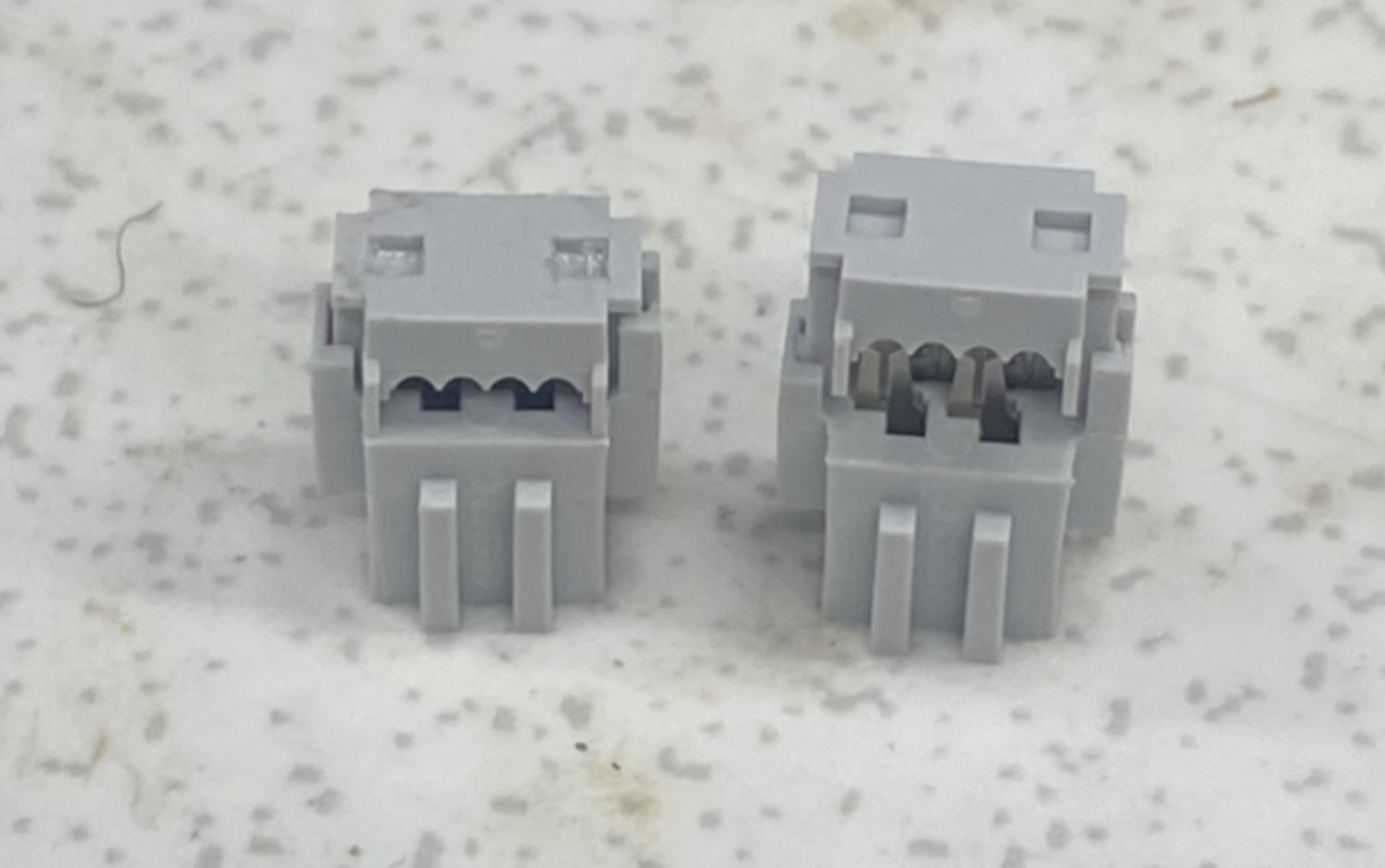
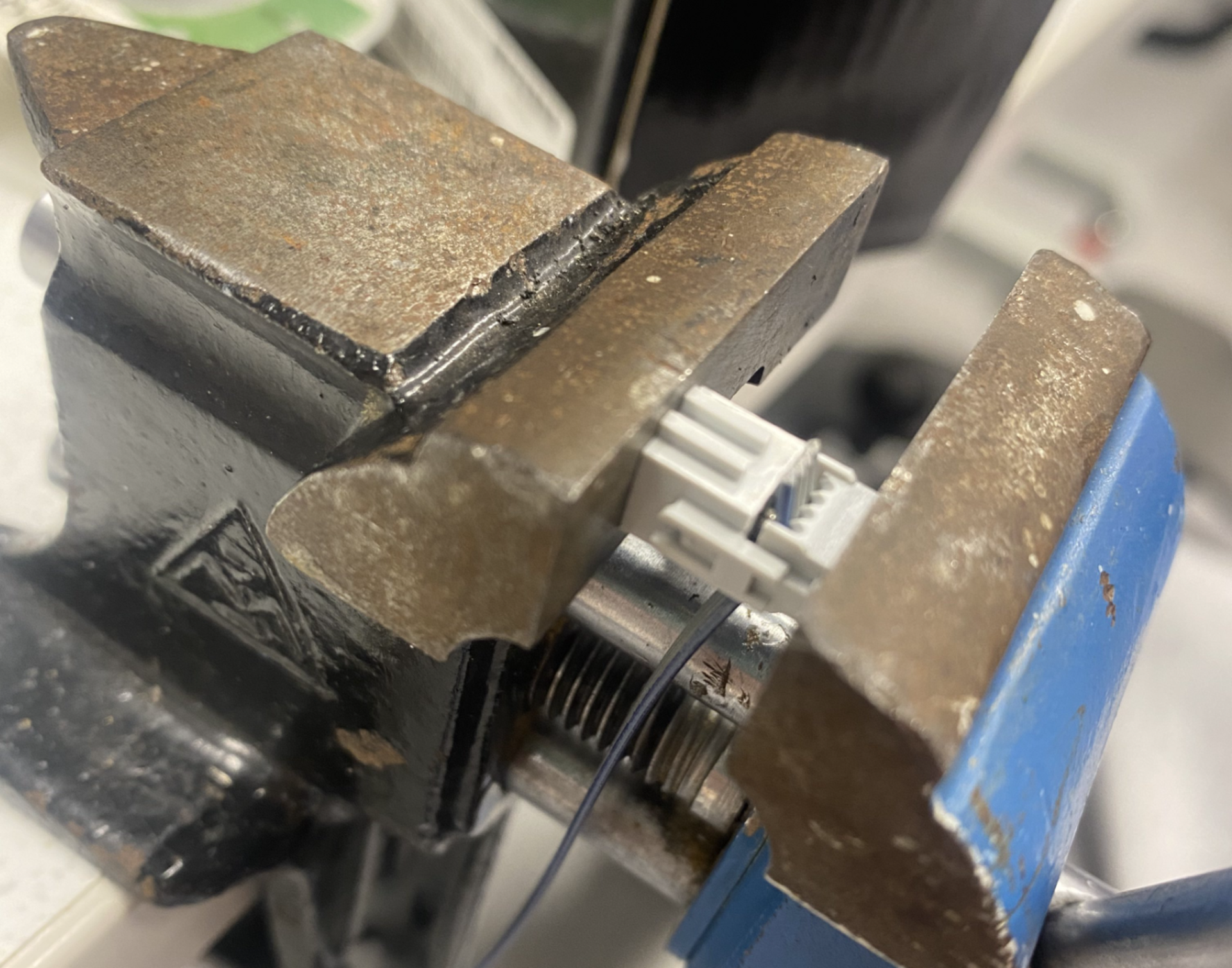
Here is the process of making the cable:
And here is the finished cable:
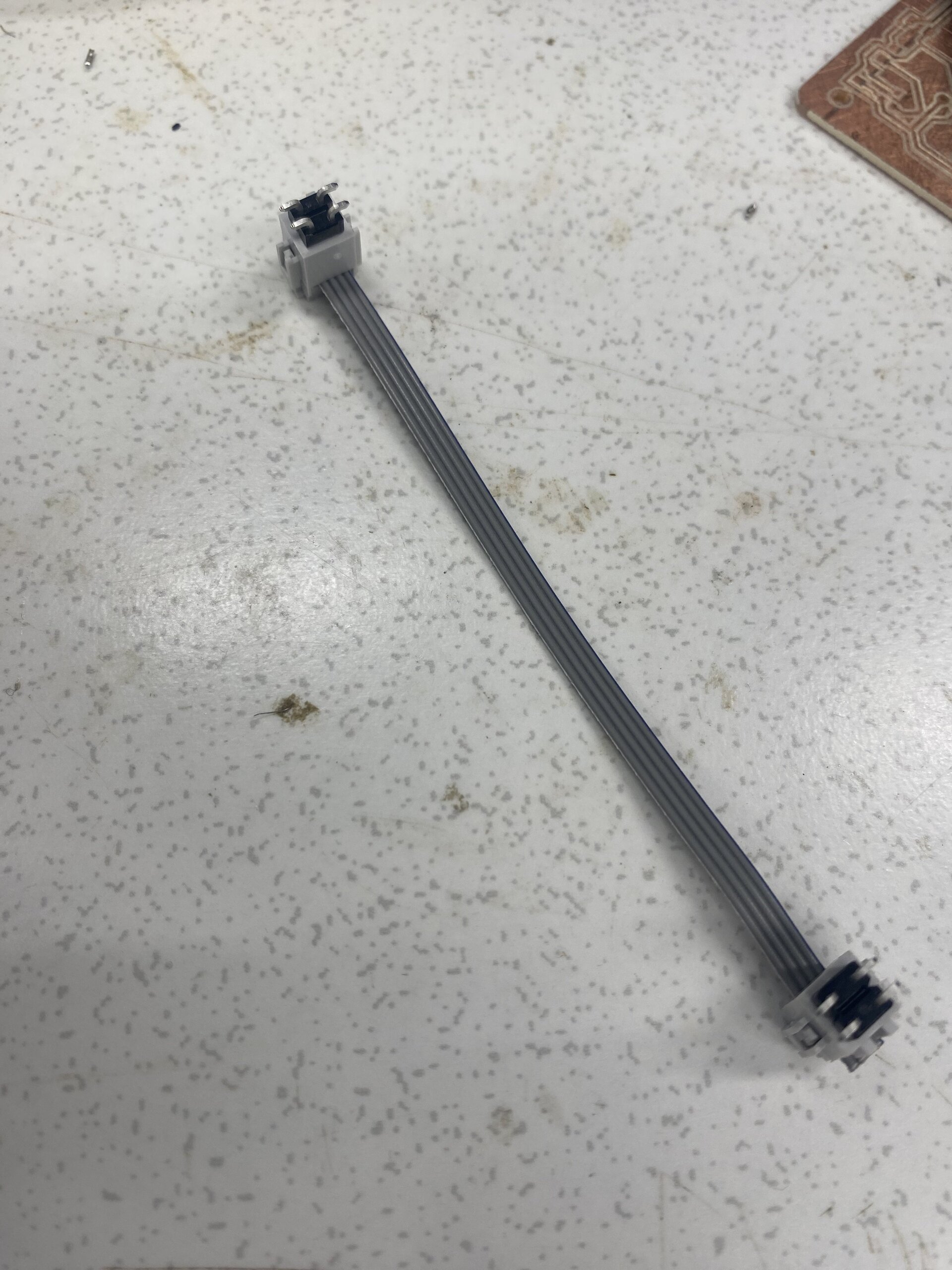
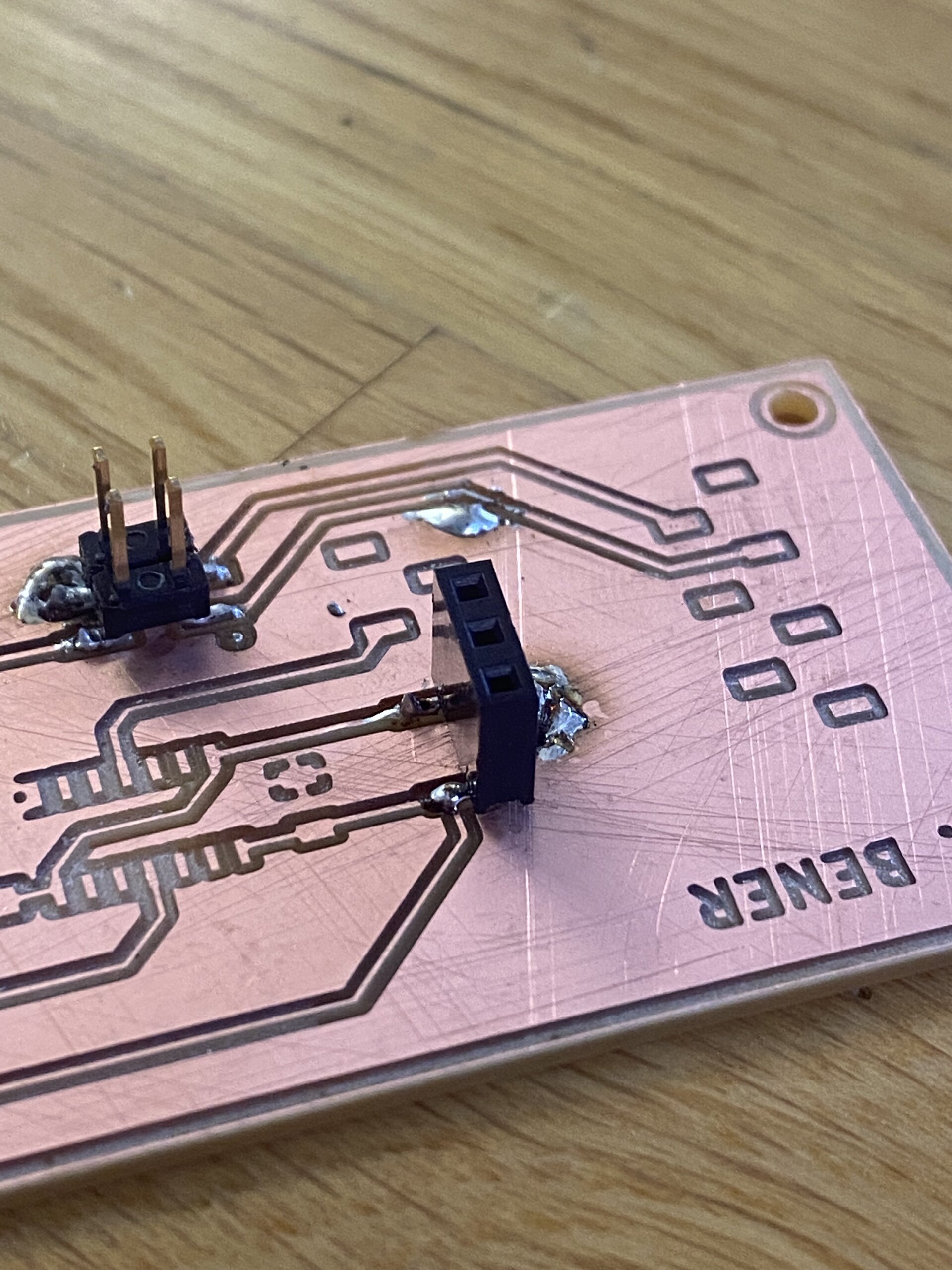
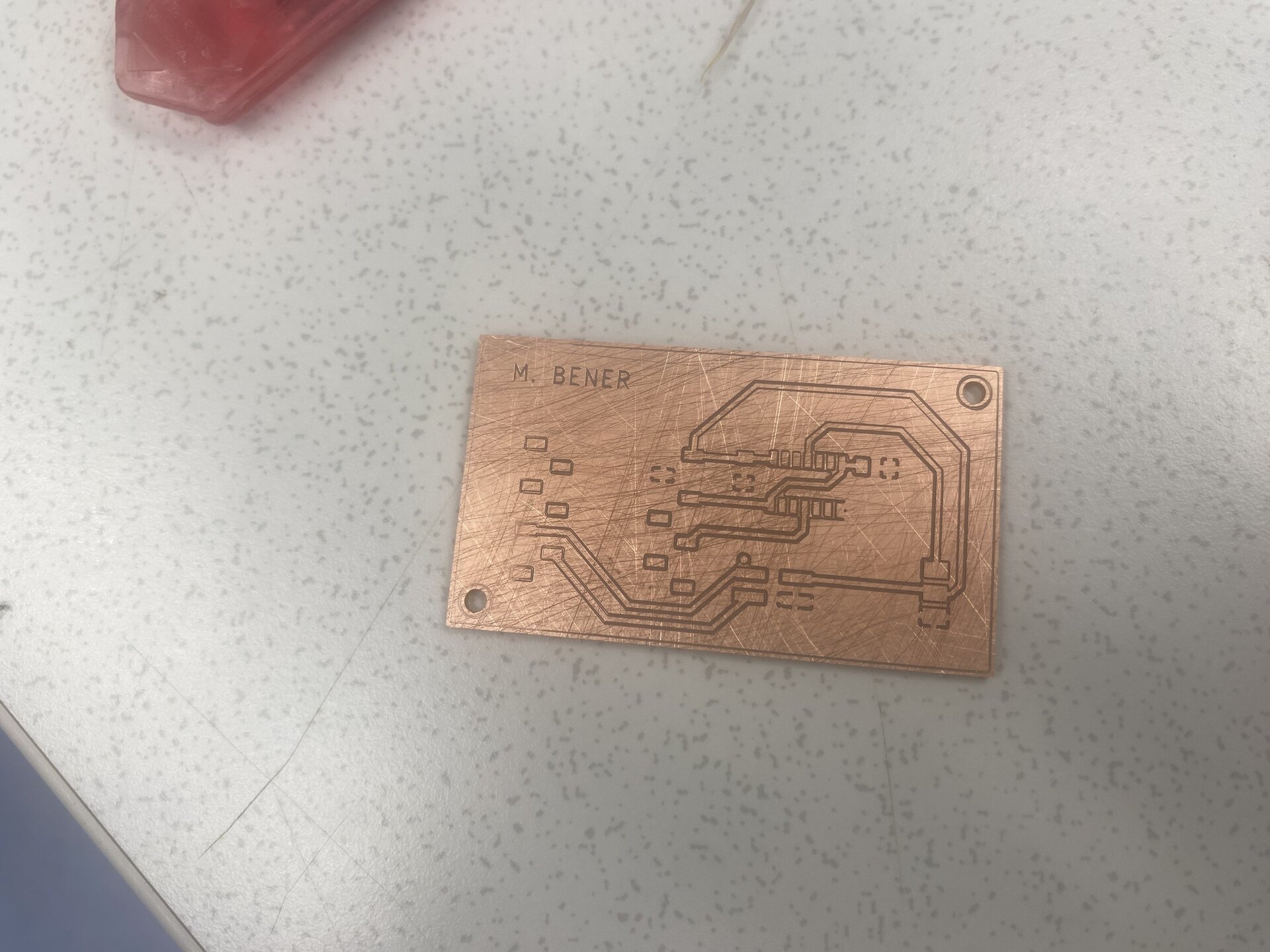
This cable is basically for the i2c communication between boards. When we connect the 2x2 pin headers in each board using this cable we can send signals over i2c to other boards. After creating the cable I moved on to laying out all my components on the board. You can see the lay’d out components on the board below:
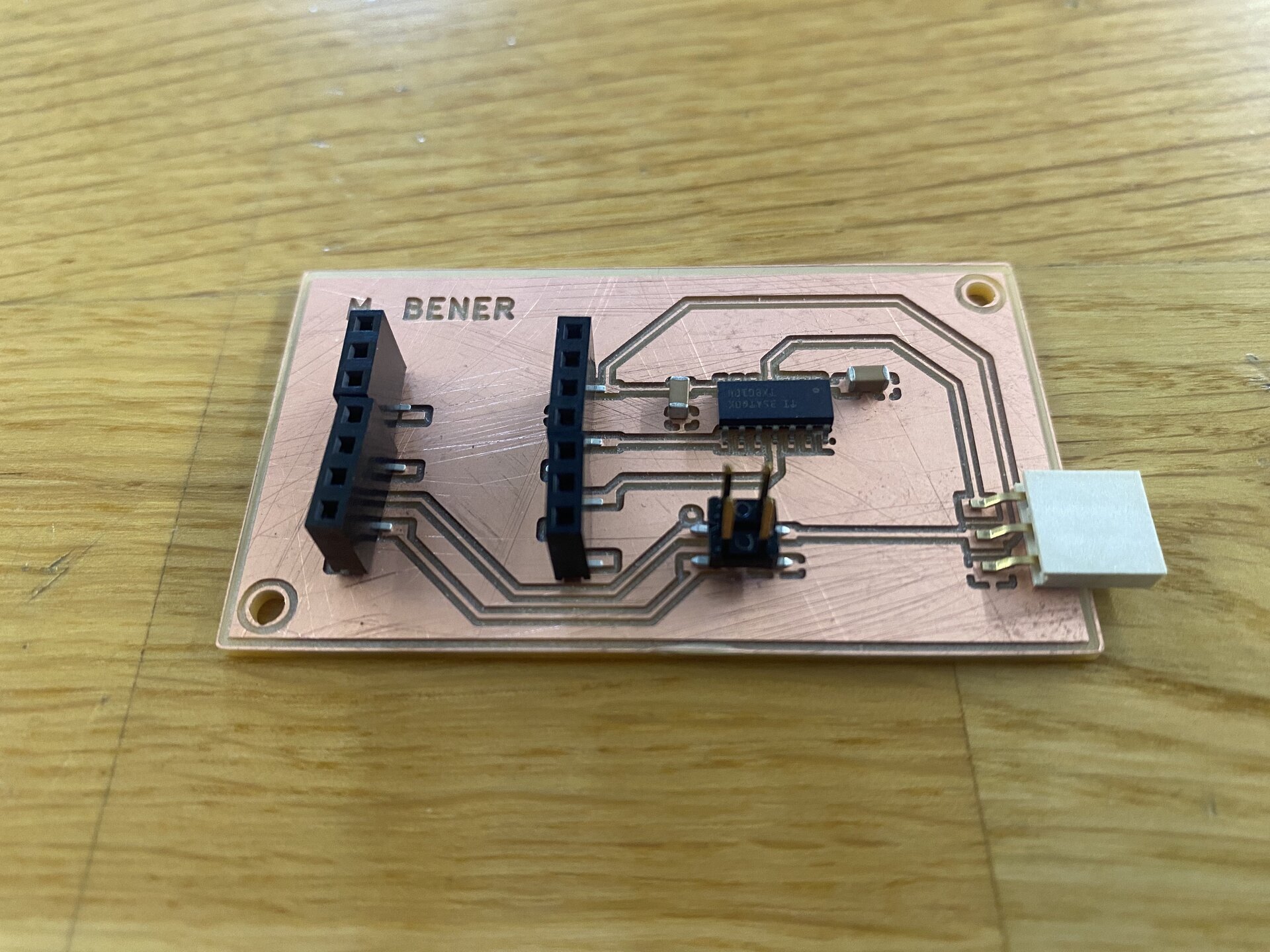
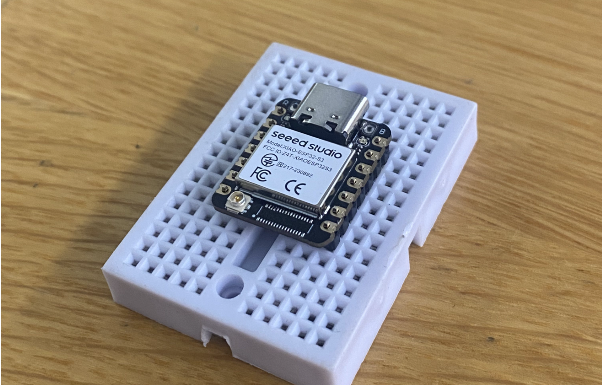
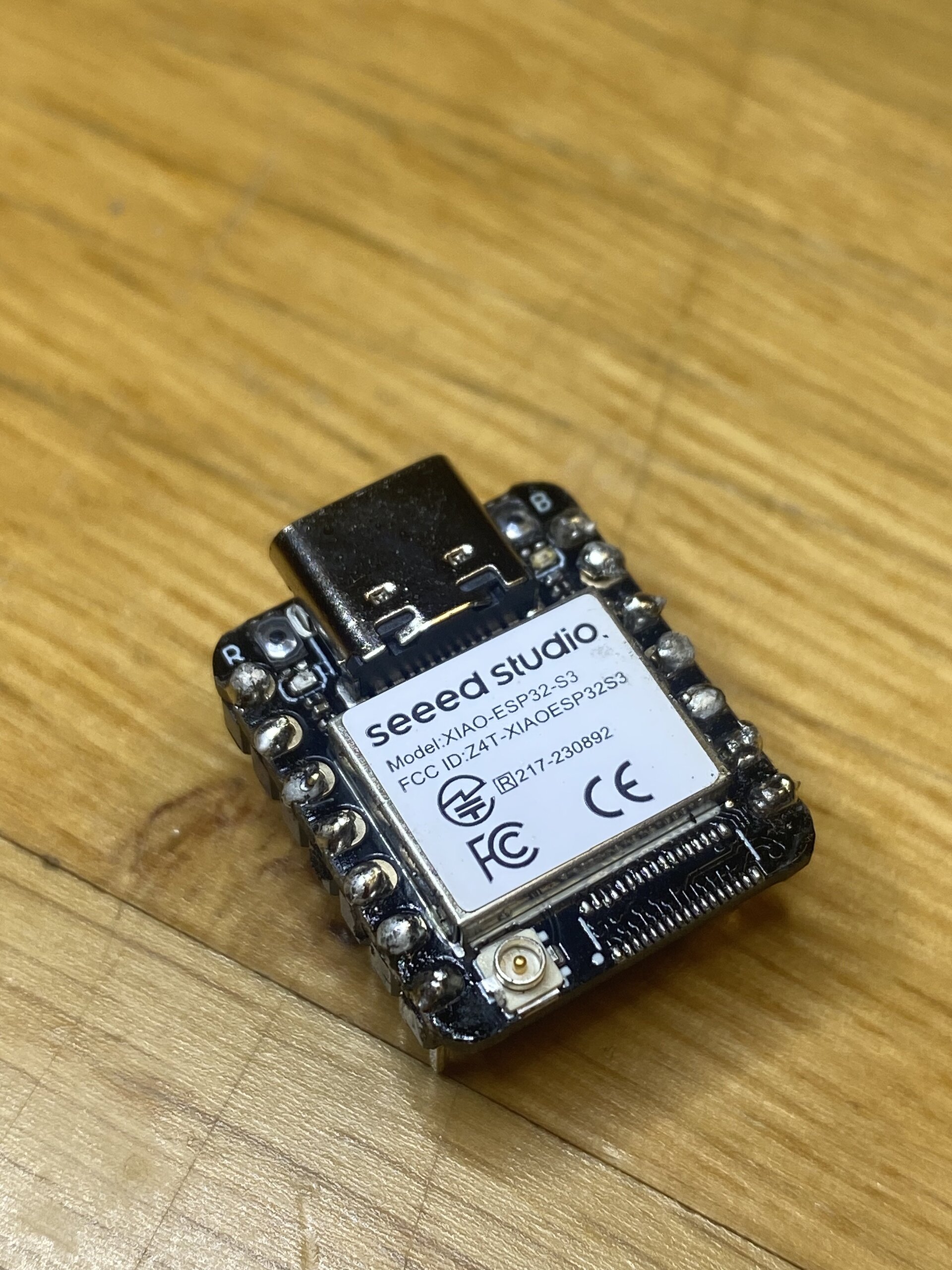
I started with the simplest soldering job: soldering the header pins onto the ESP32 microcontroller module. This involves soldering directly onto the module, not the board.
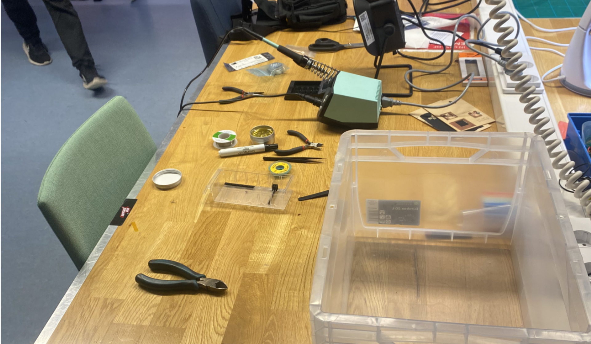
Below you can see our soldering setup:
 You can see the before:
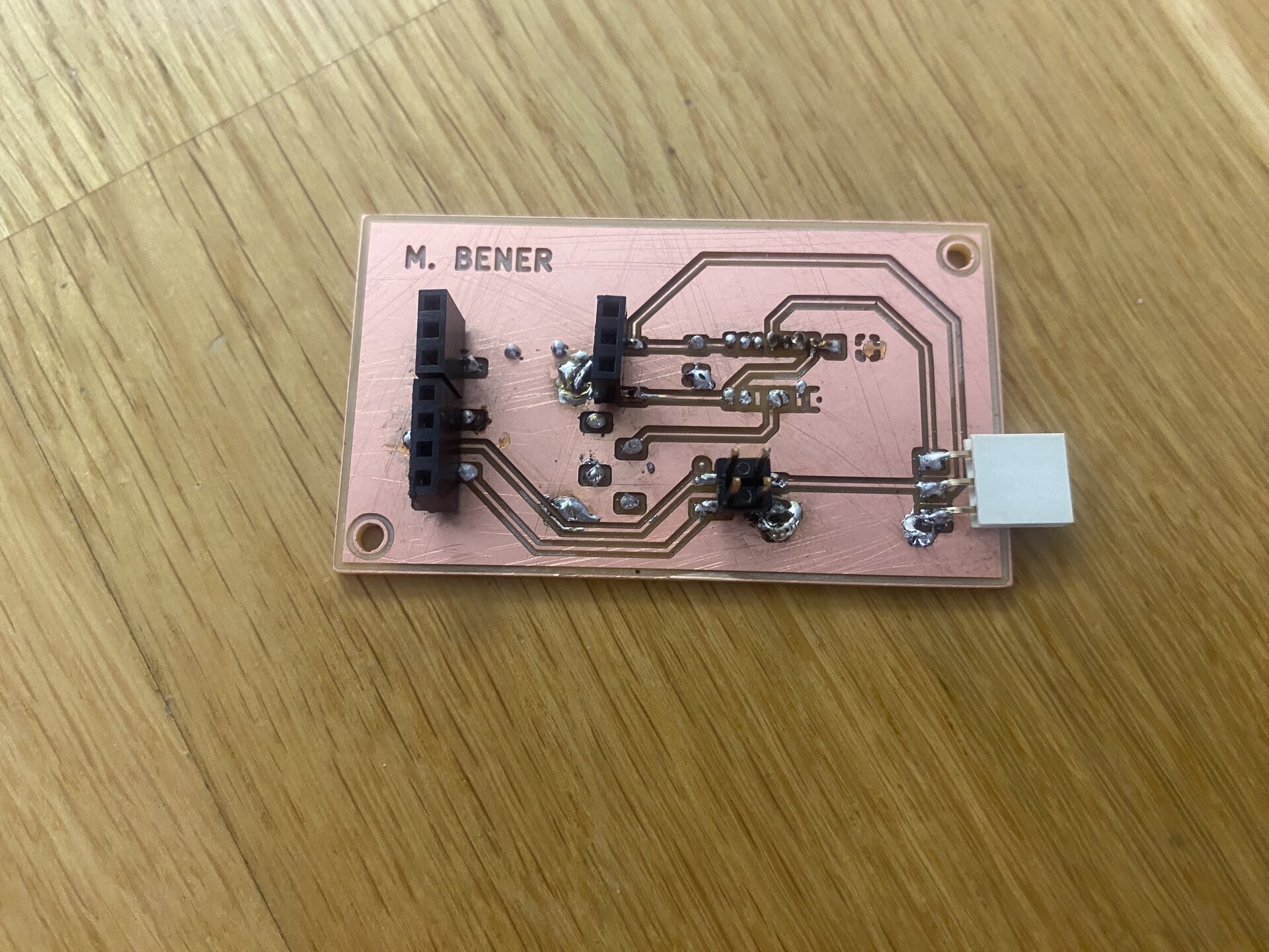
And the after:
This warmed me up for the more delicate SMD work that came next.
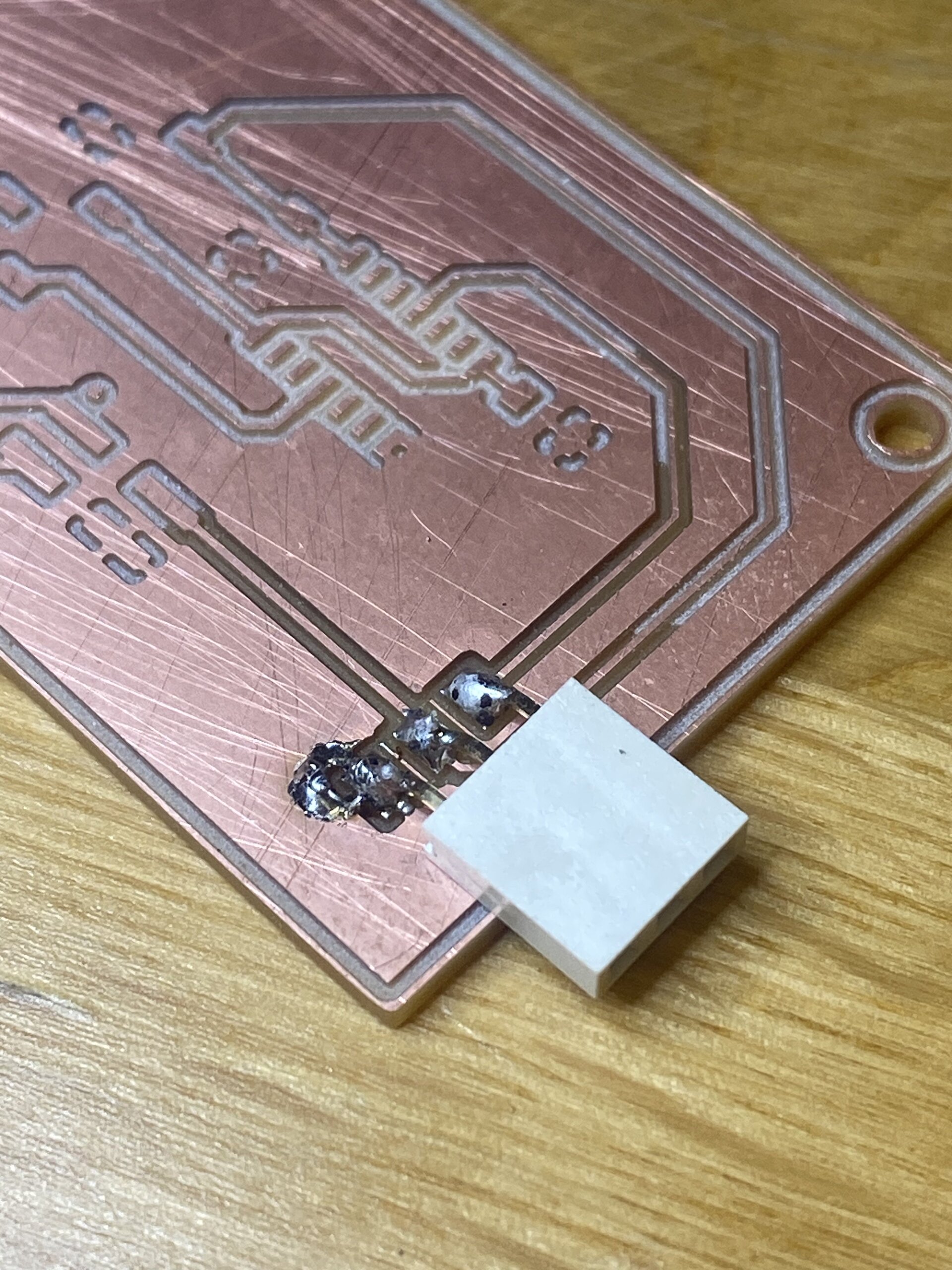
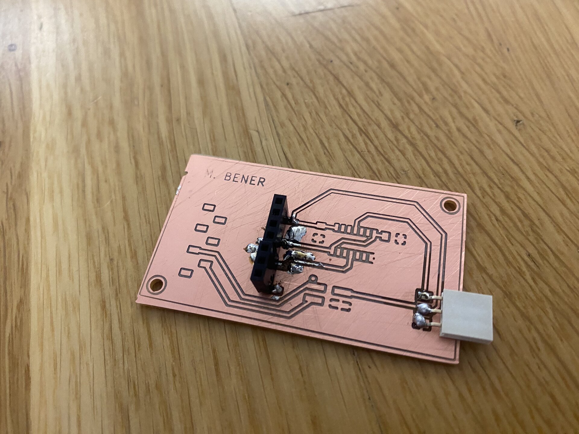
Below I soldered a 3x1 horizontal socket SMD which will be where my servo cables connect:
Below you can see my soldered 2x2 pin header that is used for i2c communication.
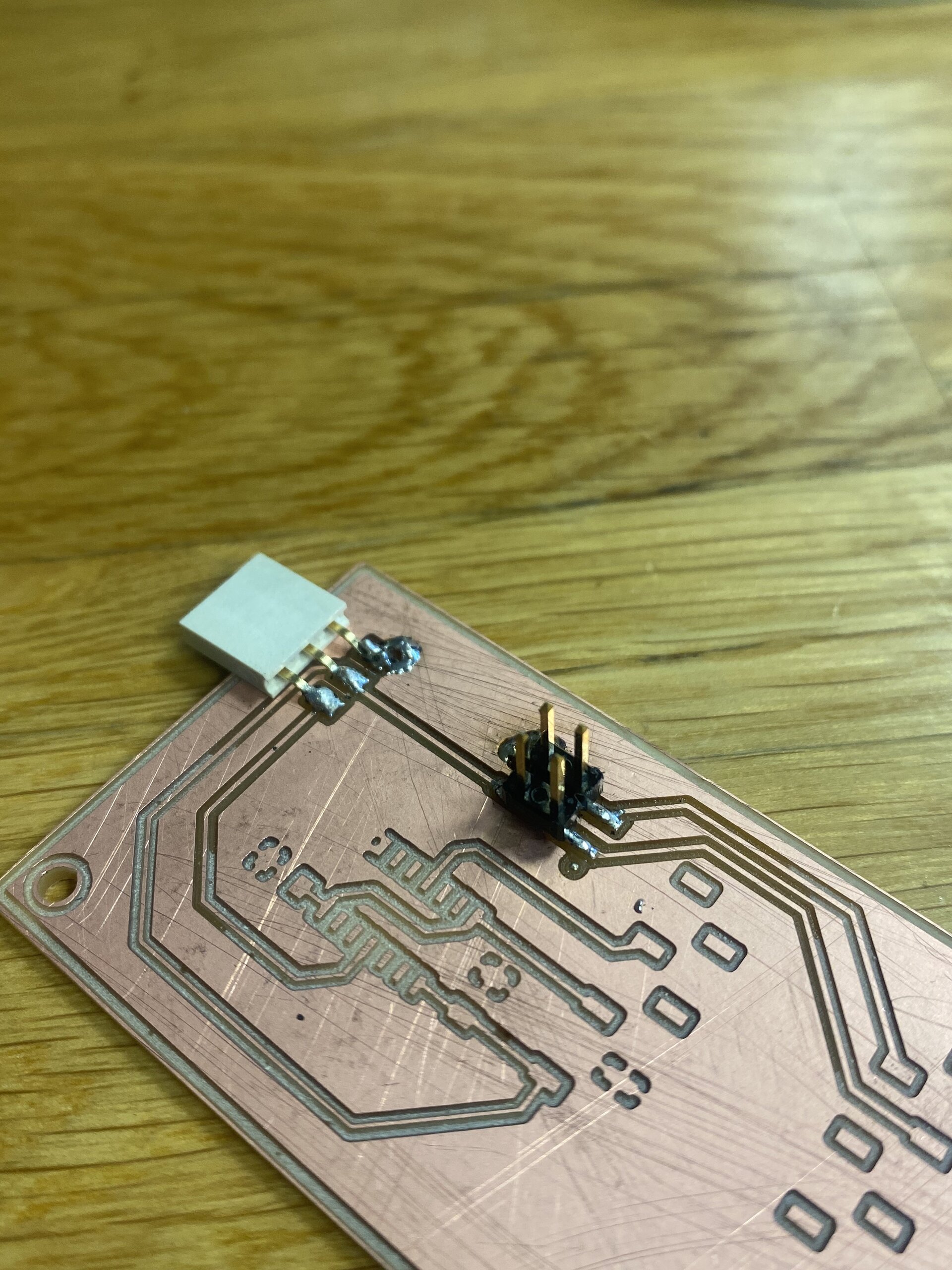
Both solders came out cleanly, and this boosted my confidence as I began working on more complex components.
I soldered the socket without paying attention to the layout, which made it impossible to add the 4×1 socket on that side. This essentially blocked part of the ESP footprint. Because of this error, I had to discard the board:
Because of this error I made my first failed board as you can see below:
My second board failed because I applied too much heat to a copper trace while trying to fix a joint, and the entire trace ripped off:
This taught me the importance of not pressing too hard with the soldering iron, not heating the same spot repeatedly and using flux to prevent overheating and tearing
And below is my third and last fail of the day where the machine couldn’t engrave some traces and plates properly.
This day was my first soldering attempt on PCB’s and SMD devices in my life so considering all of these I think it was a day I learned a lot about soldering. This day was the first day so far where we couldn’t finish the task given that day but this is normal because this was the first time we soldered PCB’s in our life and it’s a hard skill to gain that develops with experience.
The goal for tomorrow is to finish soldering a working board.