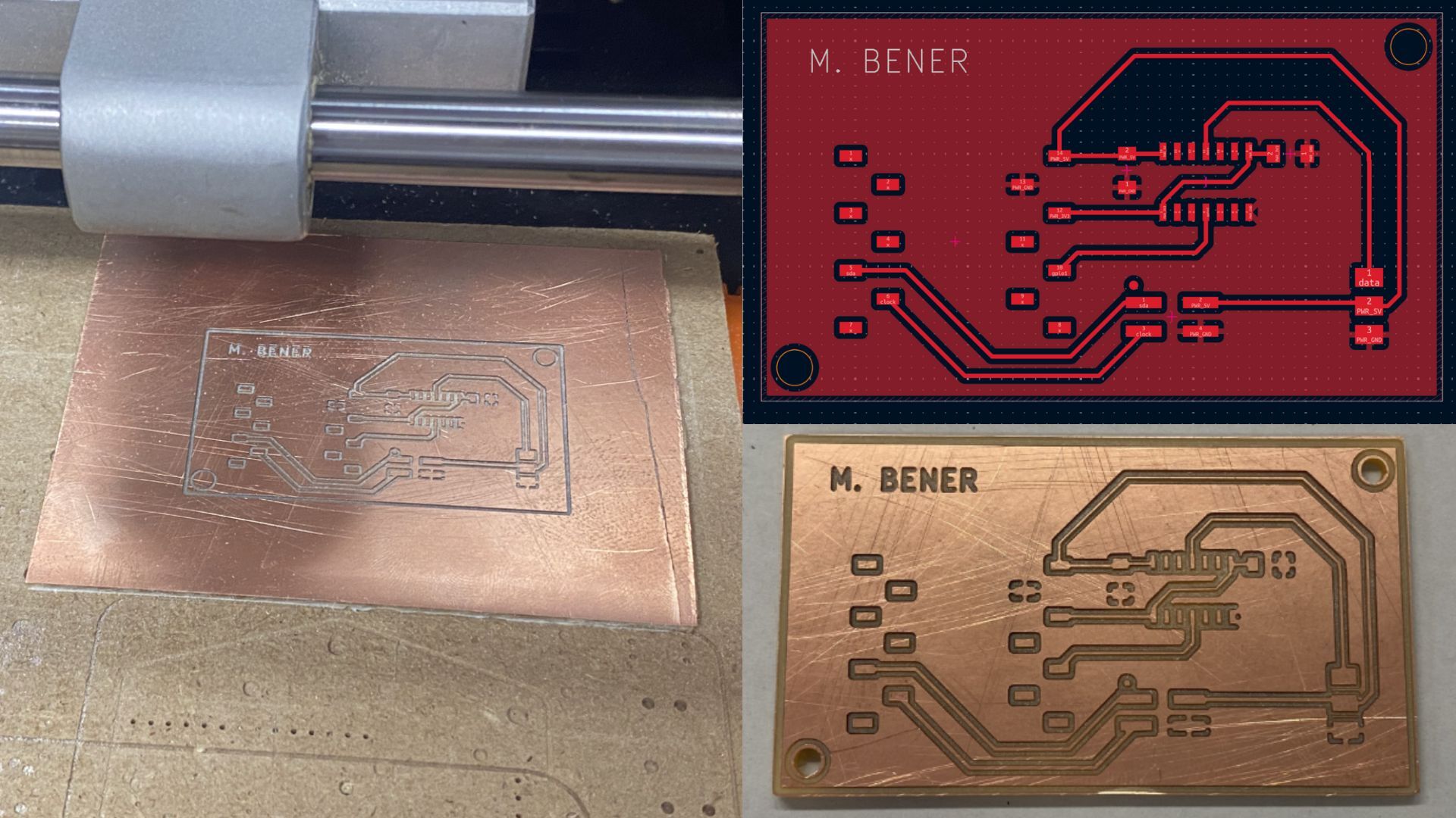
Hero Shot of the Day
Reflection at the Start of the Day
We started today at 8.00 AM. I showed my day 1 documentation to Mr. Kris to start the day and he made some comments about adjustments to my KiCad:
-
He told me to add a level shifter for the data connection of the servo. Since the servo operates at 5 V, while my ESP32-C3’s GPIO logic level is 3.3 V, Mr. Kris emphasized that the signal might not always register as a stable high. To ensure reliable communication, I needed to add a bi-directional logic level shifter converting 3.3 V to 5 V. This change would prevent weak signal highs and ensure proper PWM control for the servo.
-
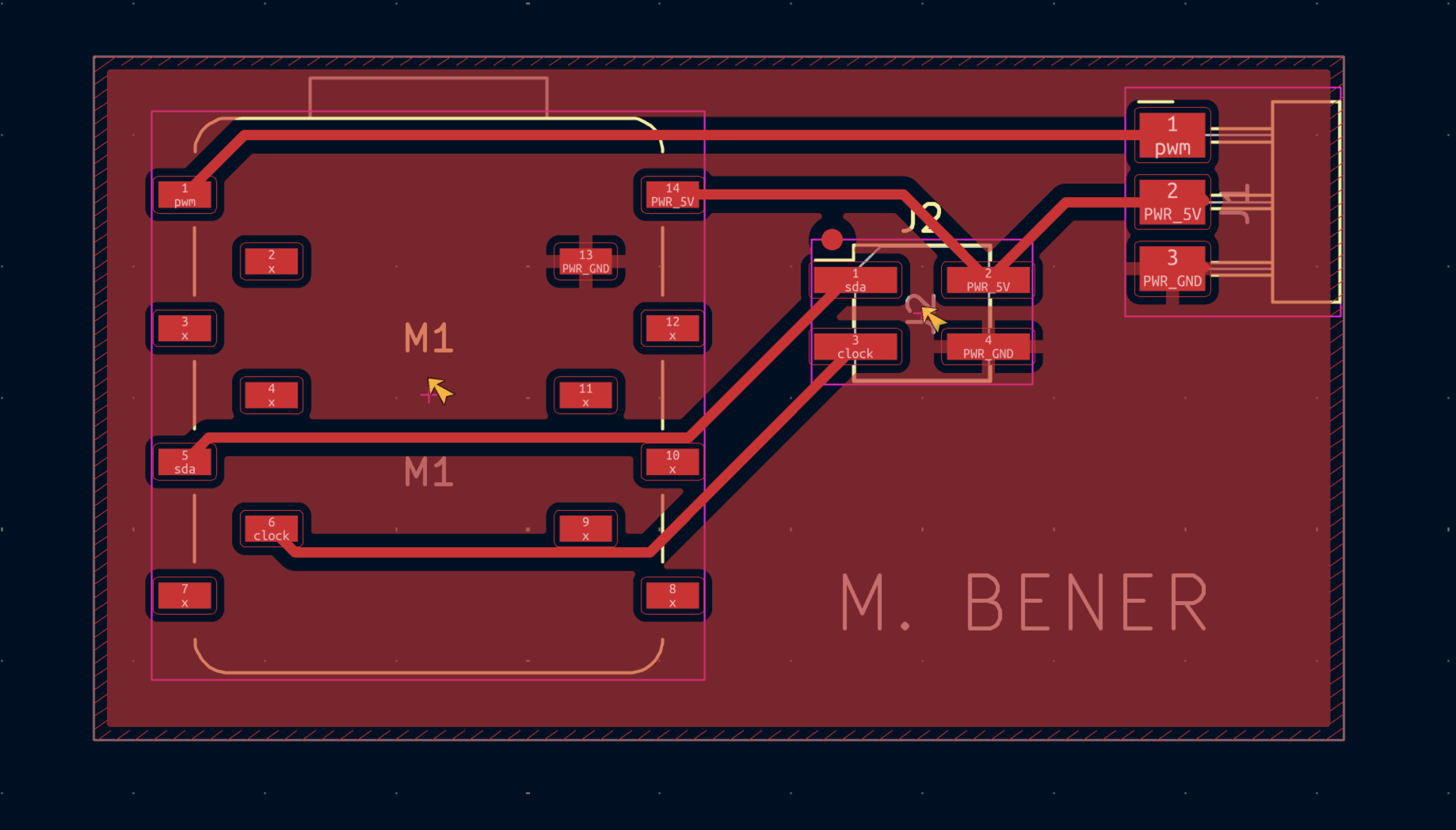
He told me about horizontal pin headers and that for the pin header to be stable, the plastic of the header should be exactly on the edge of the board. He said that for mechanical stability, the plastic of horizontal headers should align with the edge of the PCB. If the header’s plastic floats then solders can weaken over time.
Mr. Kris also gave some general tips for documentation and KiCad:
- He showed us how to add a TOC (Table of Contents) in our Obsidian documentation files.
- He showed us how to install fab library using plugins.
- He told us that only having the fab library will fasten our work process, so we deleted all other libraries. Before I experienced slowness in the workflow from the loading of the symbol and footprints libraries, so cleaning out my libraries really fastened this process. You access the menu from “Preferences”, “Manage Symbol Libraries” or “Manage Footprint Libraries”.
- He explained that to get 6x1 use two 3x1 headers. precisely snap the two headers together but this spacing isn’t correct, we need to snap together use the 2.54 mm grid thats exactly our pitch to snap the headers together. You can use the measuring tool to measure exact distance between the pins. It needs to be 2.54 mm = 0.1 inch.
So basically now I will renew my board according to Kris’s feedback so we can finalize it and mill it in the afternoon.
Renewing Board Design
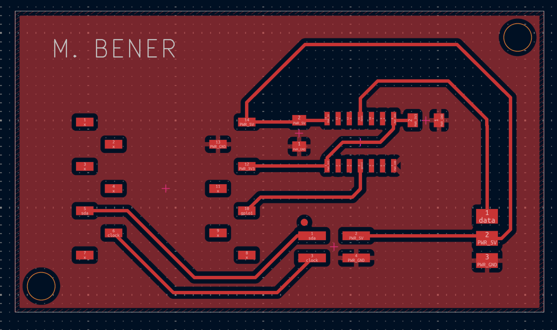
I fixed the horizontal pin headers hanging out and instability problem as you can see in the PCB design below:
Next I added a level shifter to shift the 3v3 to 5v as you can see in the schematic below:
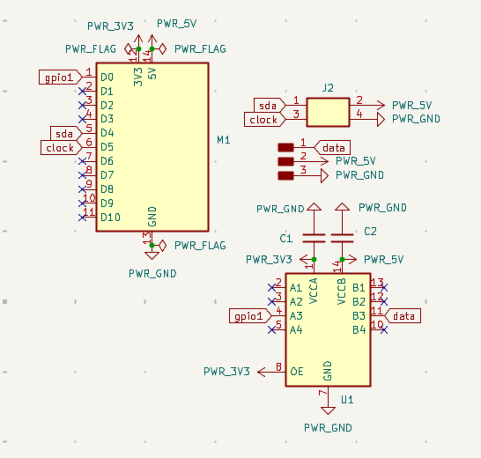
The VCCA takes an input of 3.3 Volts and uses a capacitor. The VCCB takes an input of 5 Volts and uses a capacitor. The GND is connected to the common ground while I give a constant high signal to the Tri-State output mode enable. I use A3 as an input 3.3 Volt signal and B3 as an output 5 Volt signal to give to the servo data.
Next I made the PCB design as you can see below:
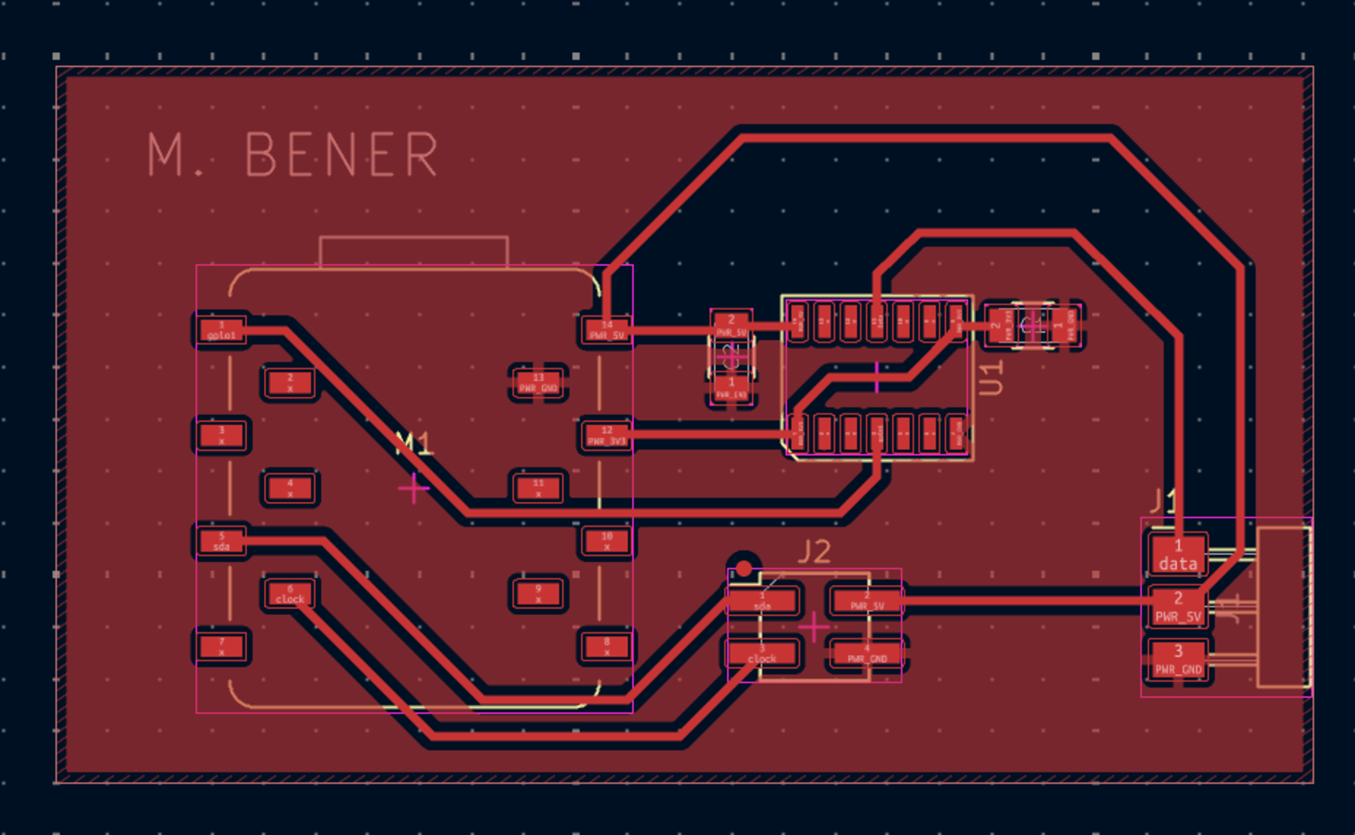
I made sure that no GND was separate from the common ground and I made sure that all tracks were 0.4 mm and that the production would be easier with no solders that are too close. I made sure that the ERC and DRC didn’t have any errors and no important warnings.
Then adding screw holes to my PCB came to my mind so I quickly added them:
Now it was time to show Mr. Kris my final board design, if approved then I will move on to milling.
PCB Milling
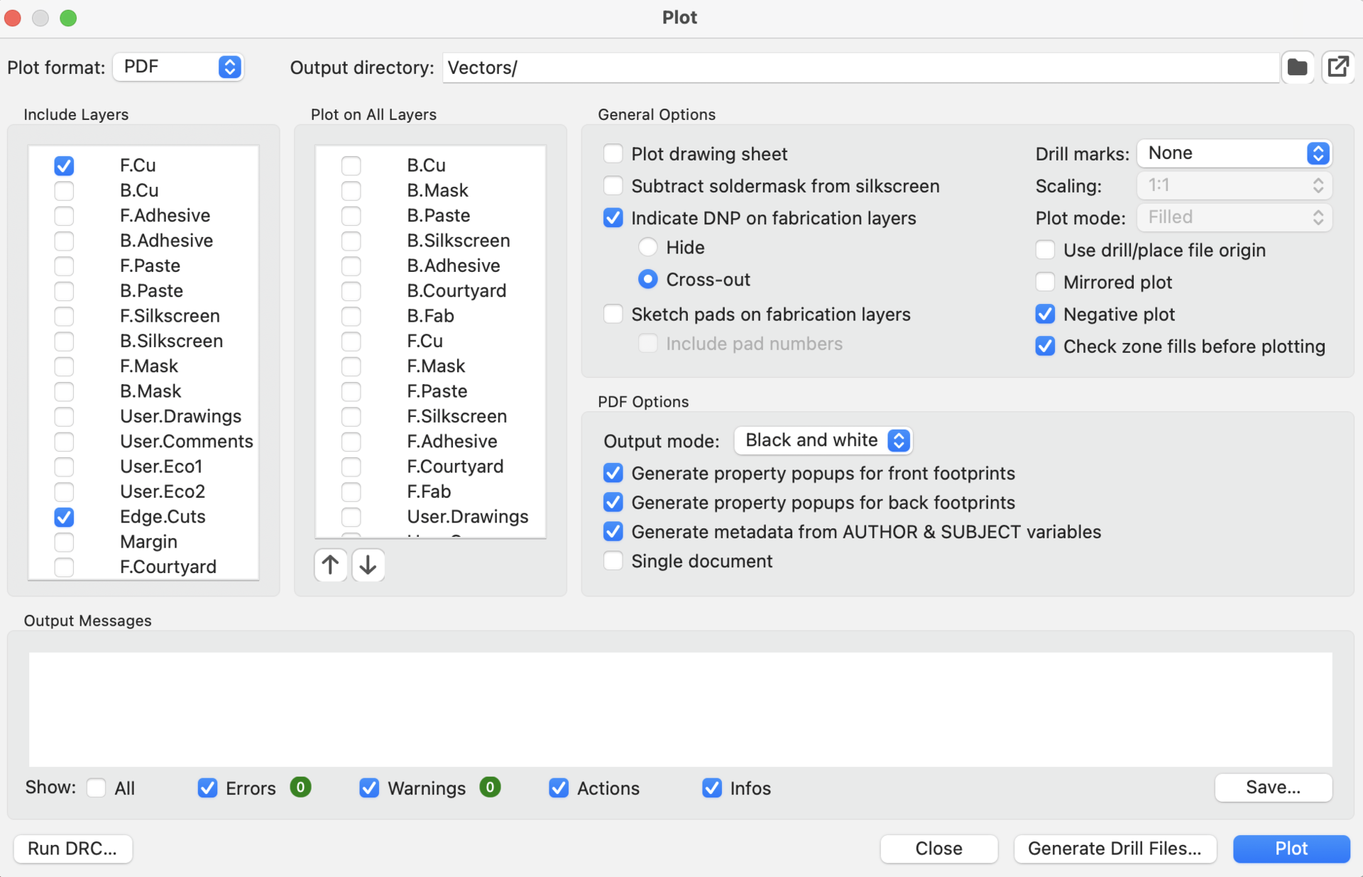
First we need to export our KiCad design as a PDF. We export four separate PDF’s:
- The copper layer
- The edges layer
- The user1 layer with the name
- The drill layer with the mounting holes
You can see the plot menu below to export pdf’s. We export with negative plot checked. The reason we don’t export SVG’s is because the KiCad SVG export is broken. So we first export PDF then transfer it to SVG using Inkscape.
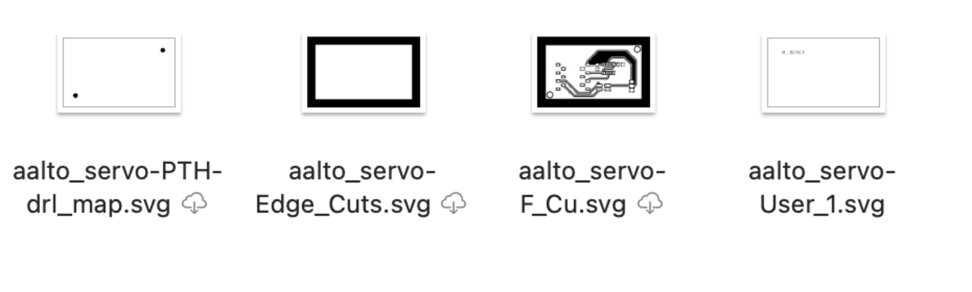
The svg files can be seen below that are exported from Inkscape. In Inkscape I resized and changed color and exported as svg as you can see below. I resized the pdfs all to the same size while I changed the colors from black to white in the drill map and text for the software to recognize the black parts as the milling parts.
 Below you can find the https://modsproject.org/ website’s page for the programs, open program, Roland SRM-20 mill, Mill 2D PCB. You can see the UI layout below. We start by uploading the svg of the layer.
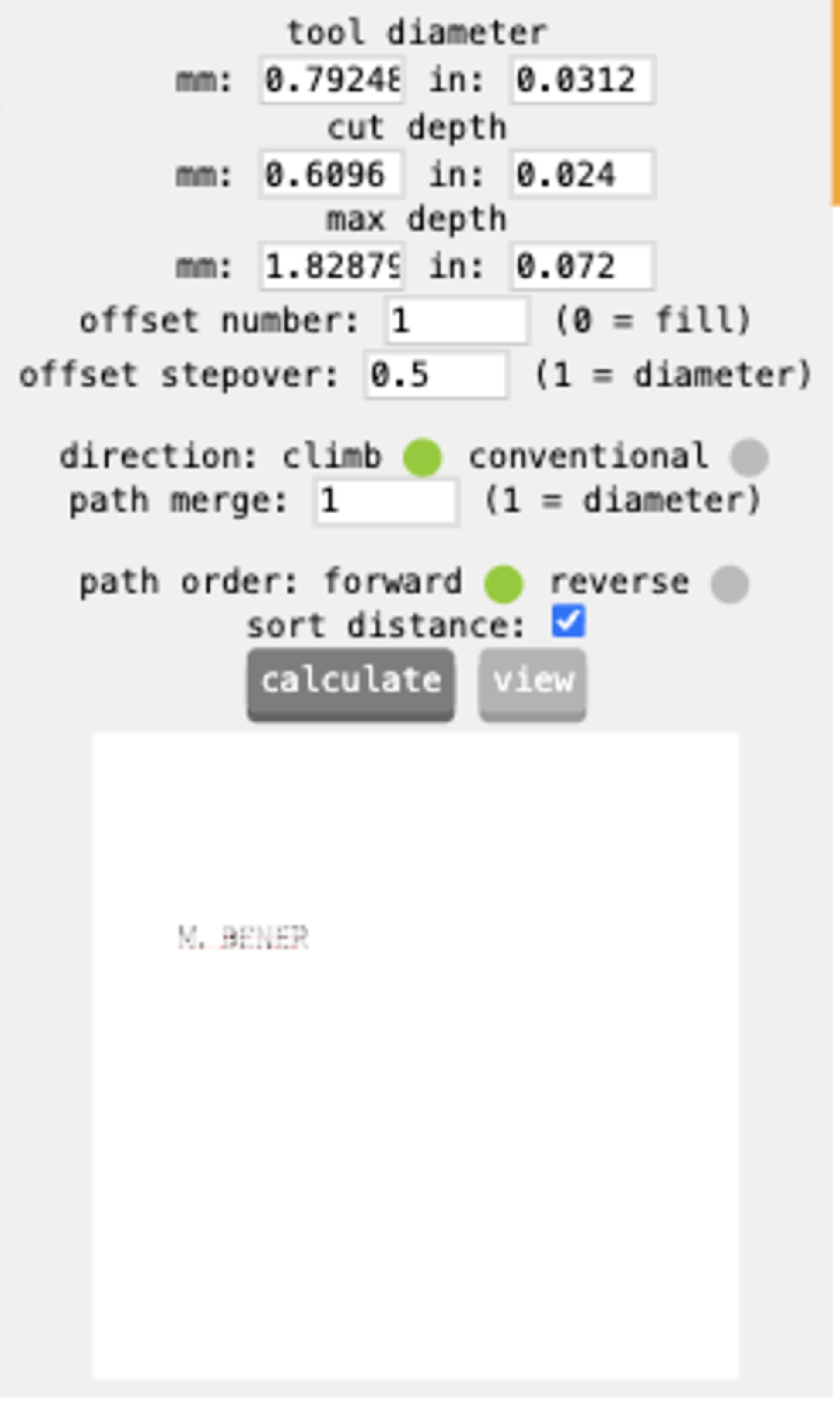
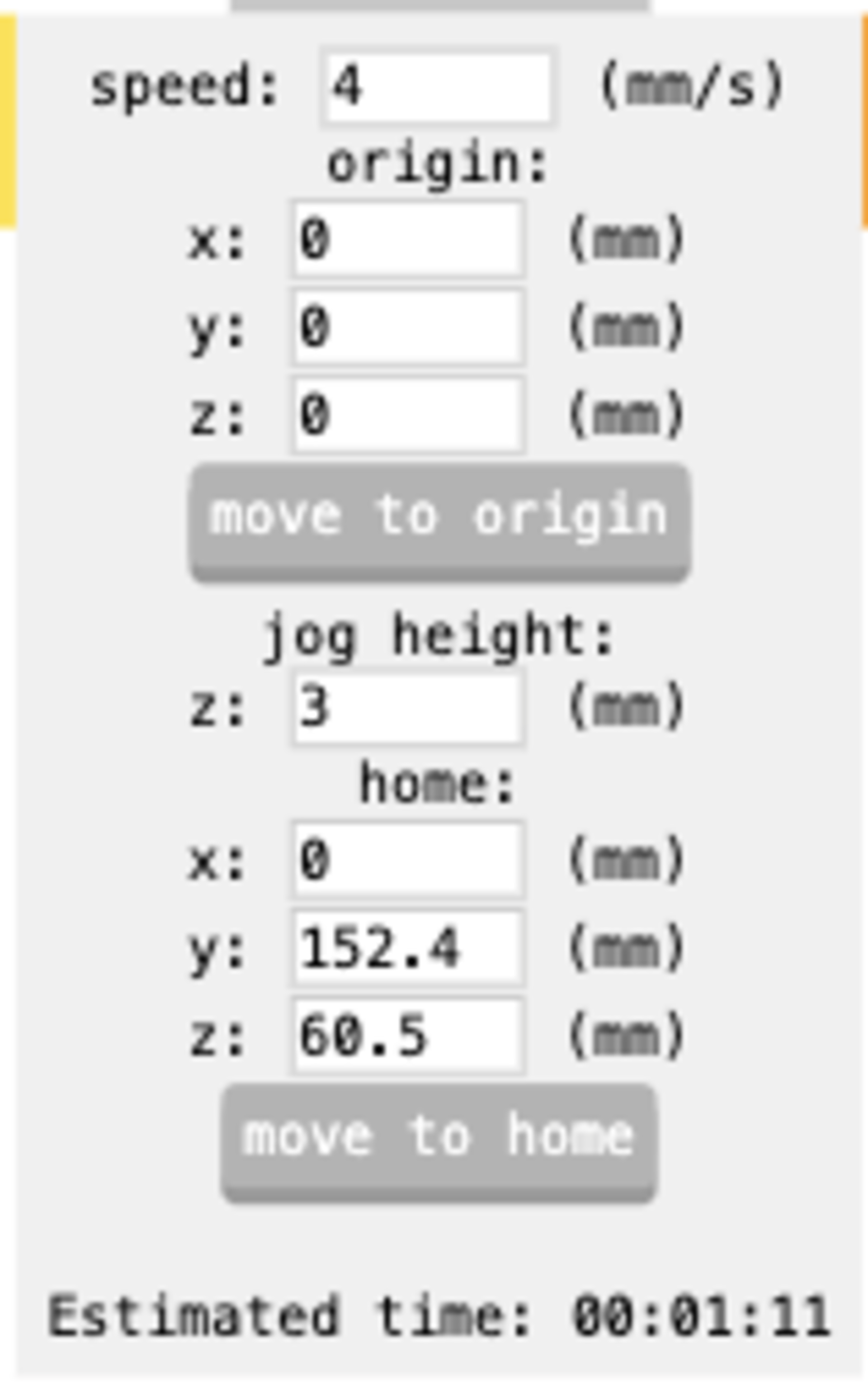
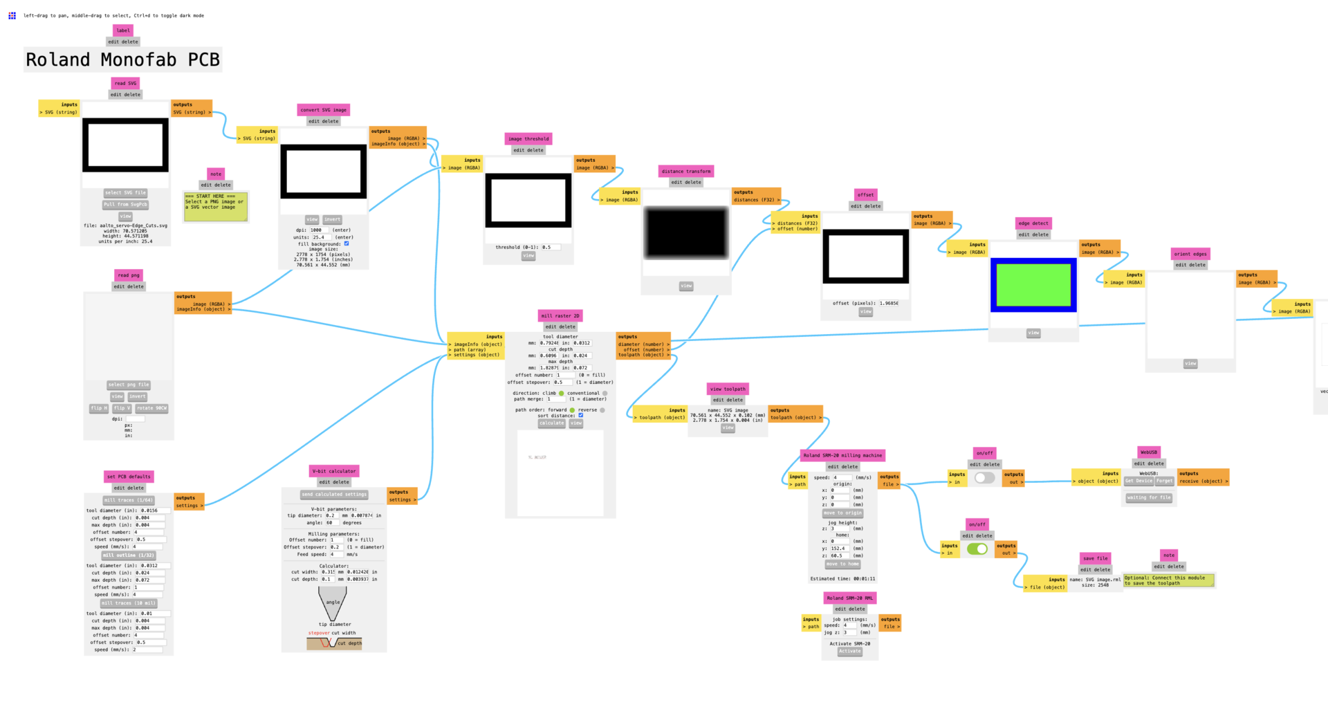 Below you can see the values we use when adjusting for the machine in the website.
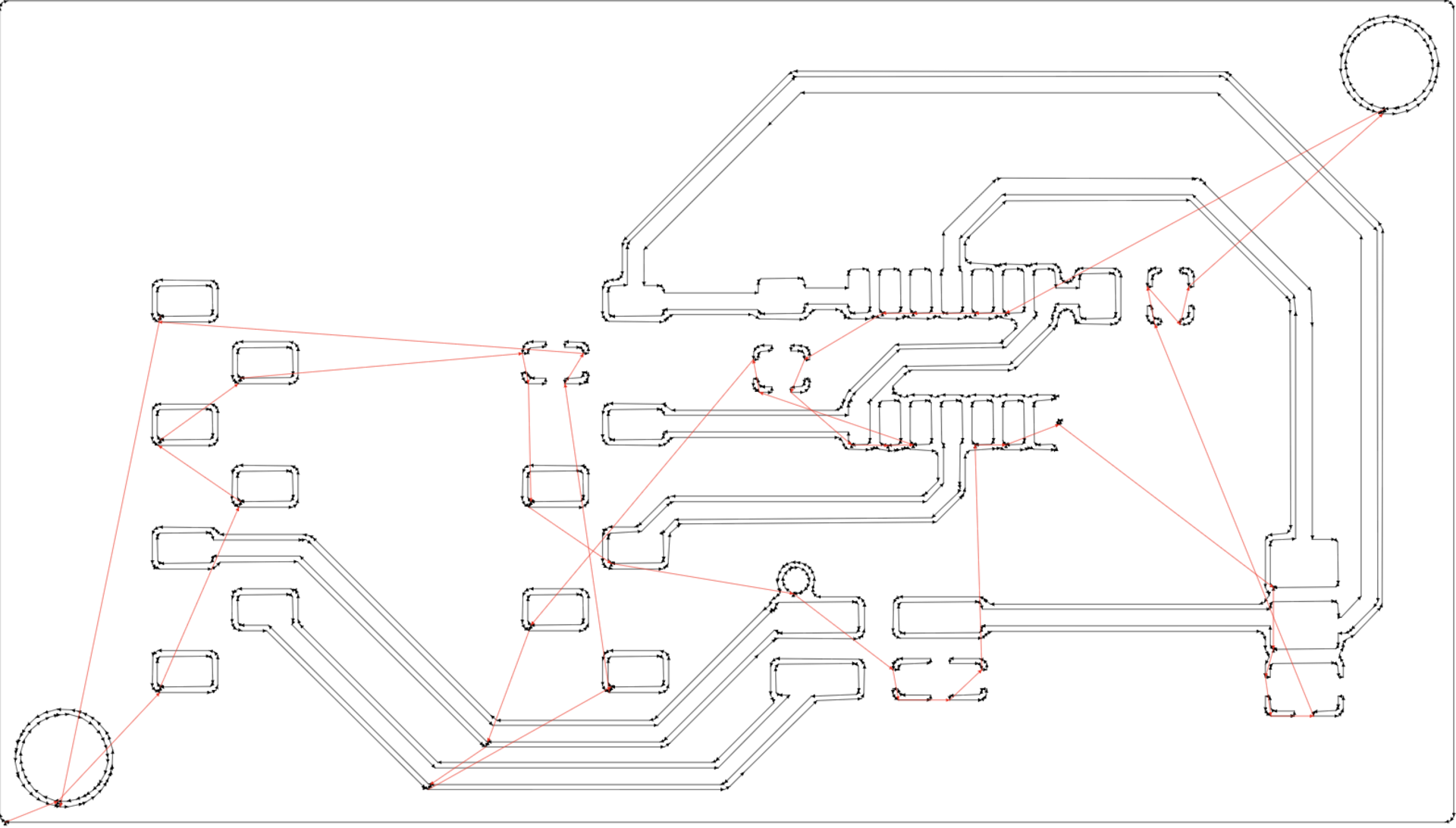
Below is an example output for the copper layer:
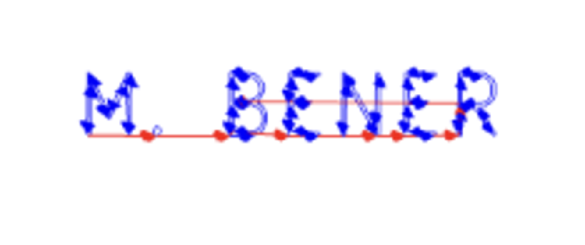
Below is an example output for the user1 layer for the name engraving:
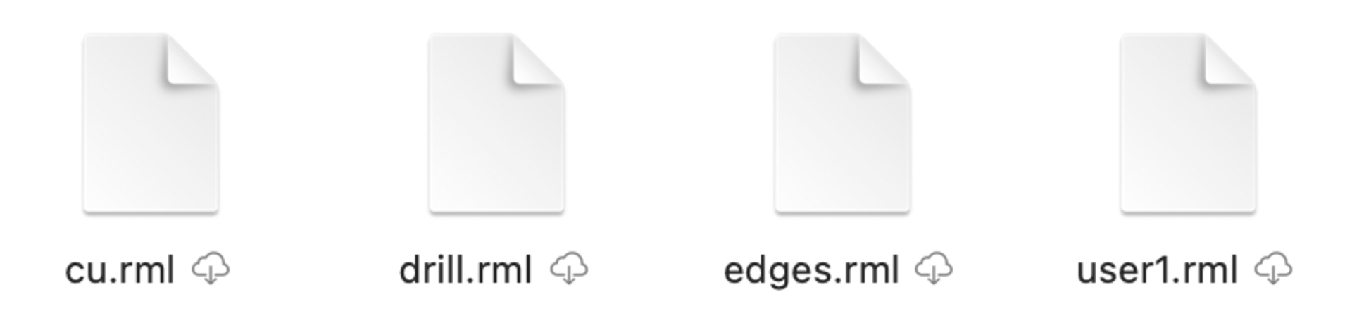
 Below are the output files we send to the Windows machine:
 Here are some notes about the errors we faced and how we solved them during the .rml file production:
- In the mods editor ui the default origin is (10, 10, 10) mm so during my first mill it milled air. So I changed the origin point to (0, 0, 0) for it to mill properly.
- Also the offset number was 4 for the copper layer (ENGRAVING LAYER) initially and this is wrong as it should be just 1 showing it cuts 1 time. So basically for cutting we only need the offset number to be 1 but for engraving it can be 4.
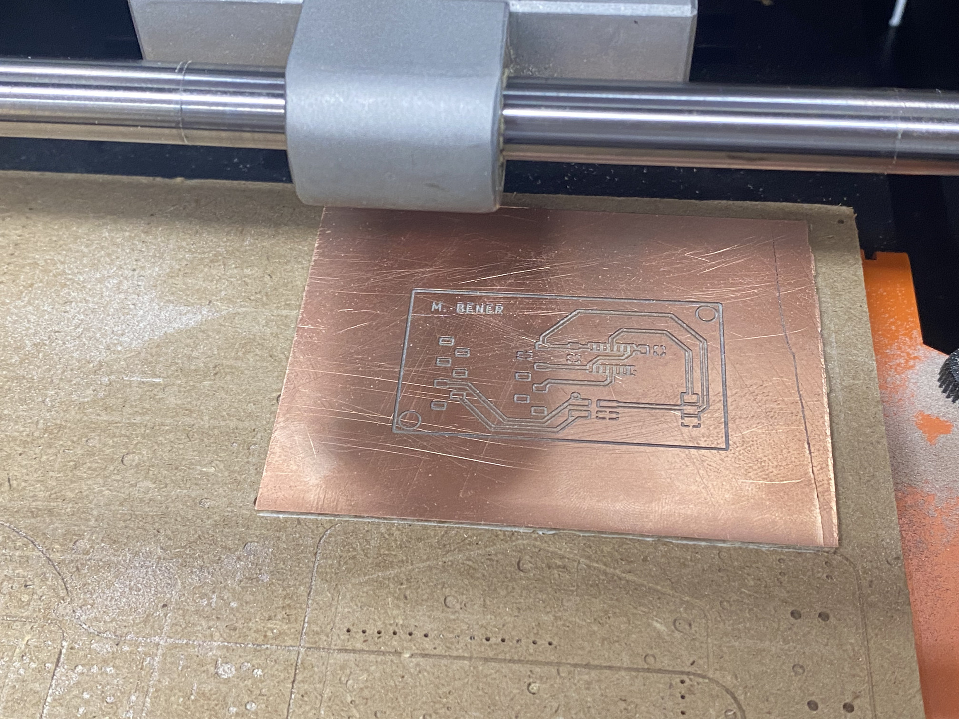
For the milling part we start with taping the copper clad with double sided tape:
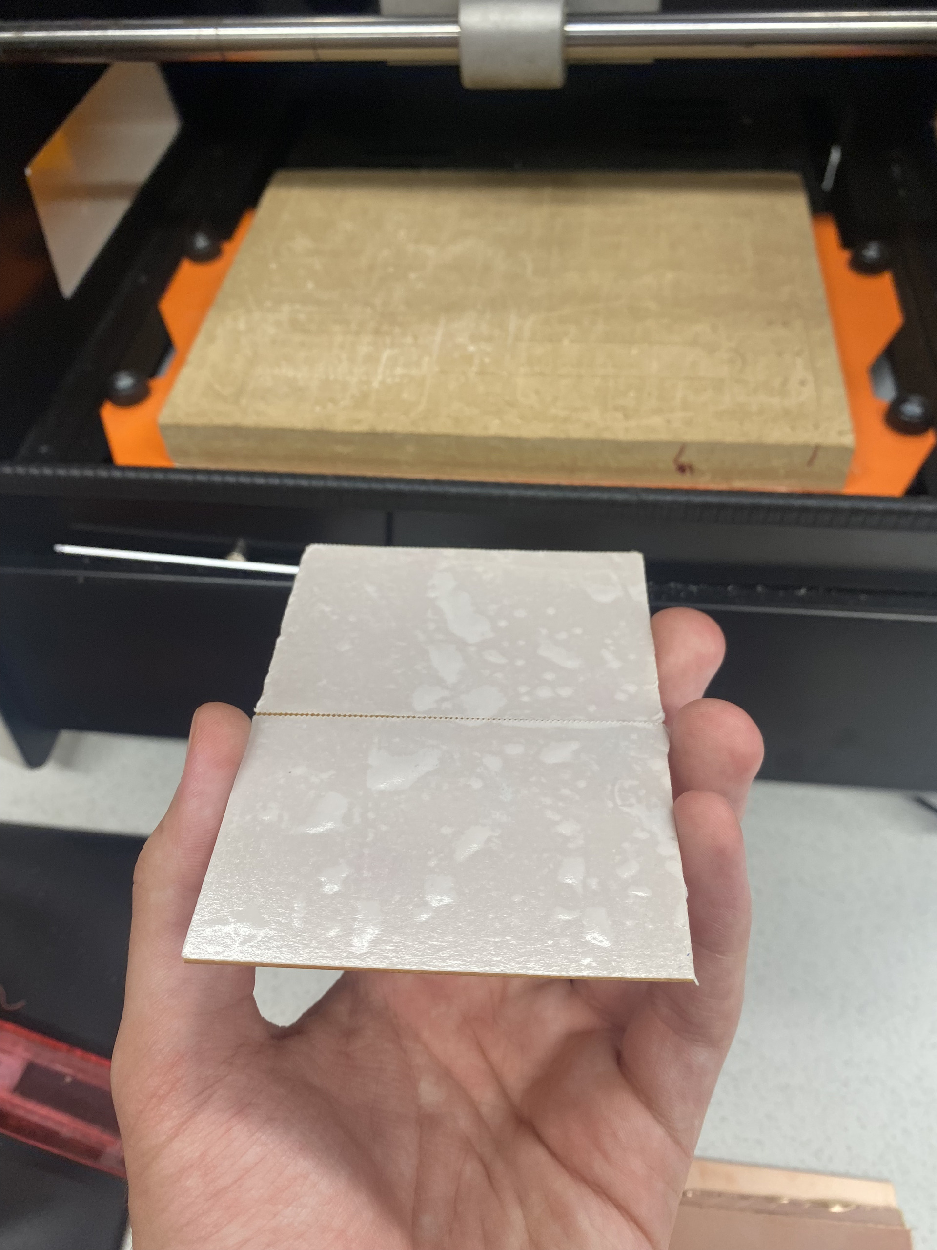
Here is taped copper clad:
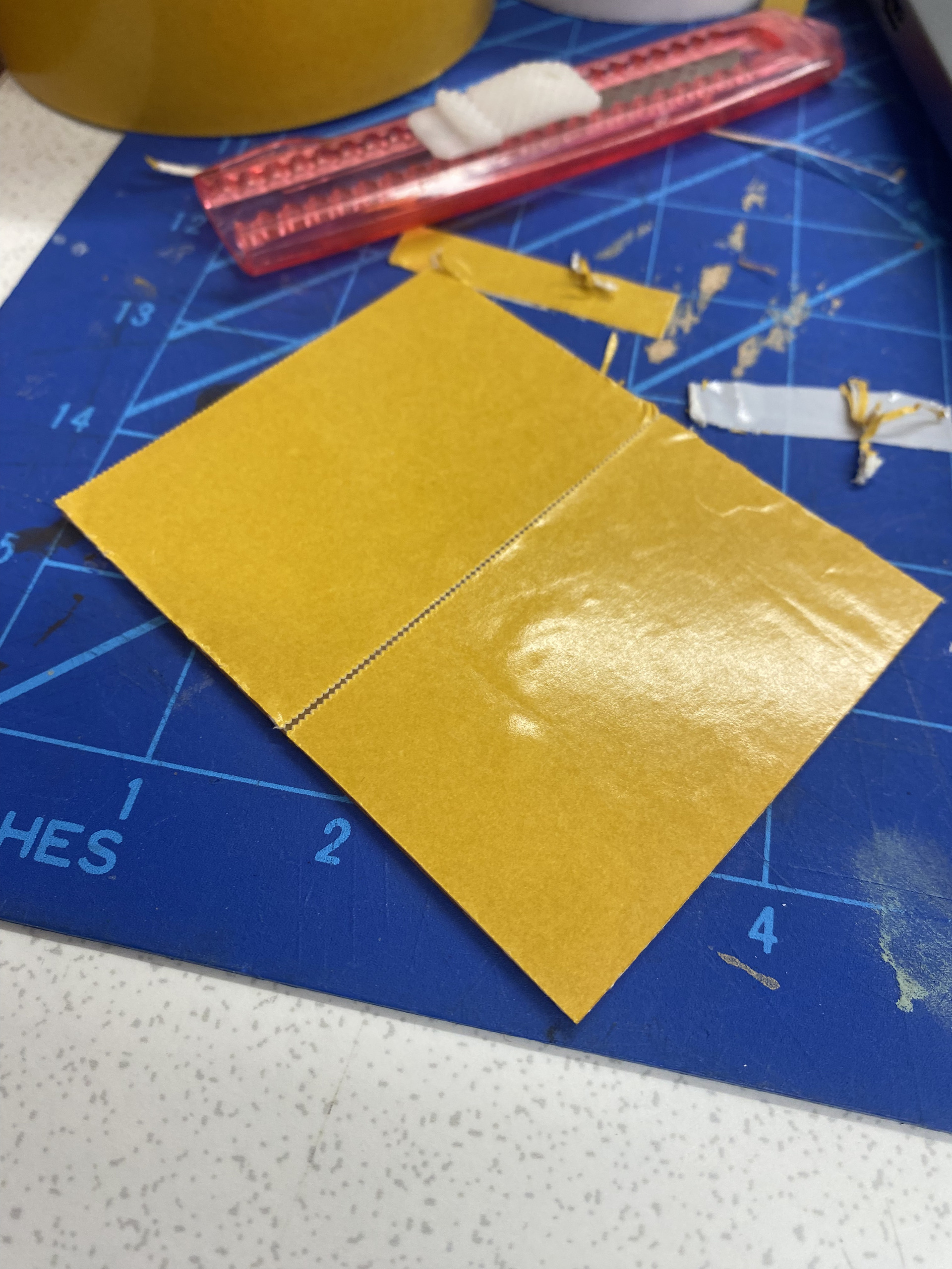
Then we tape the copper clad inside our machine as seen below:
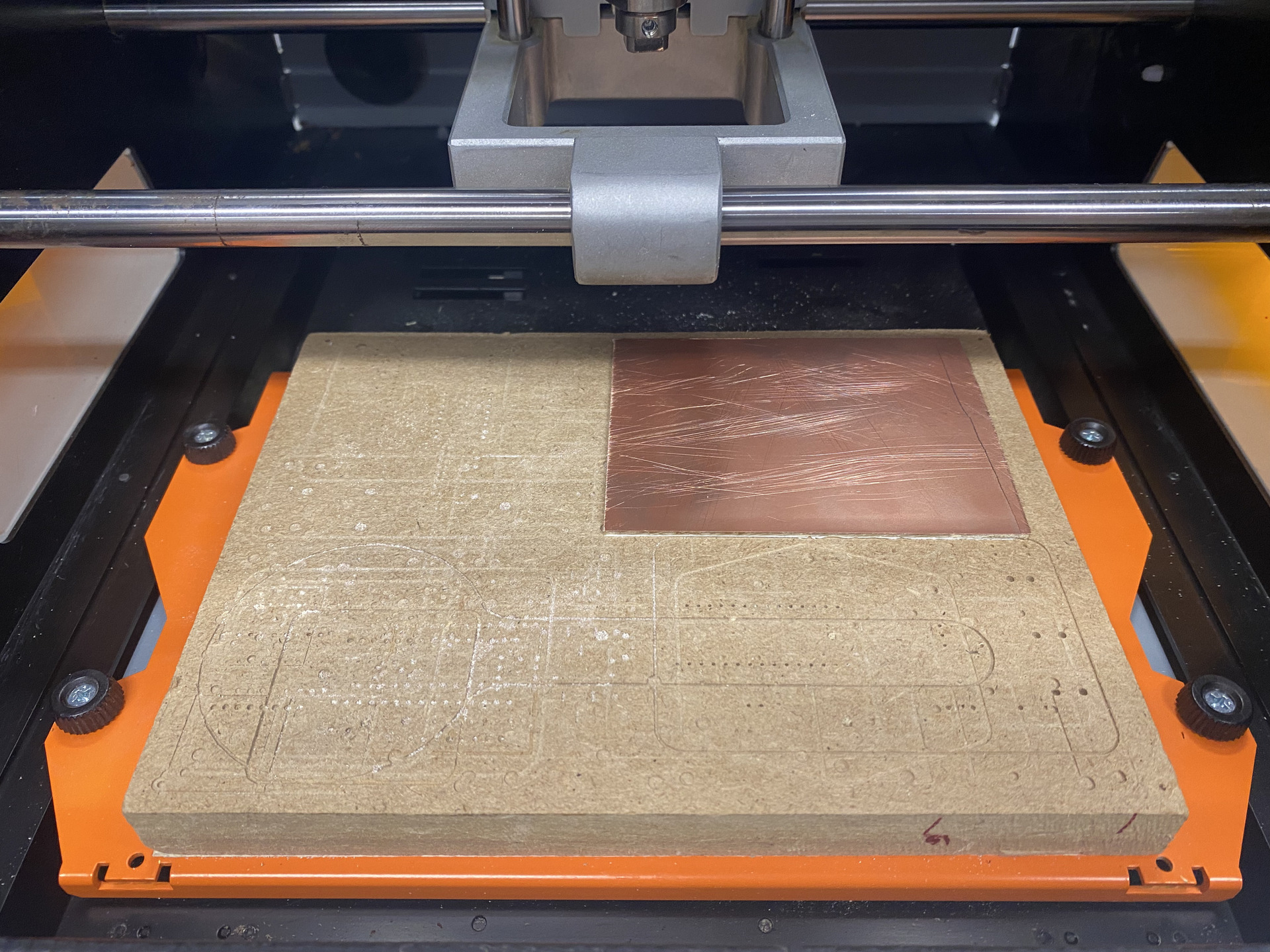
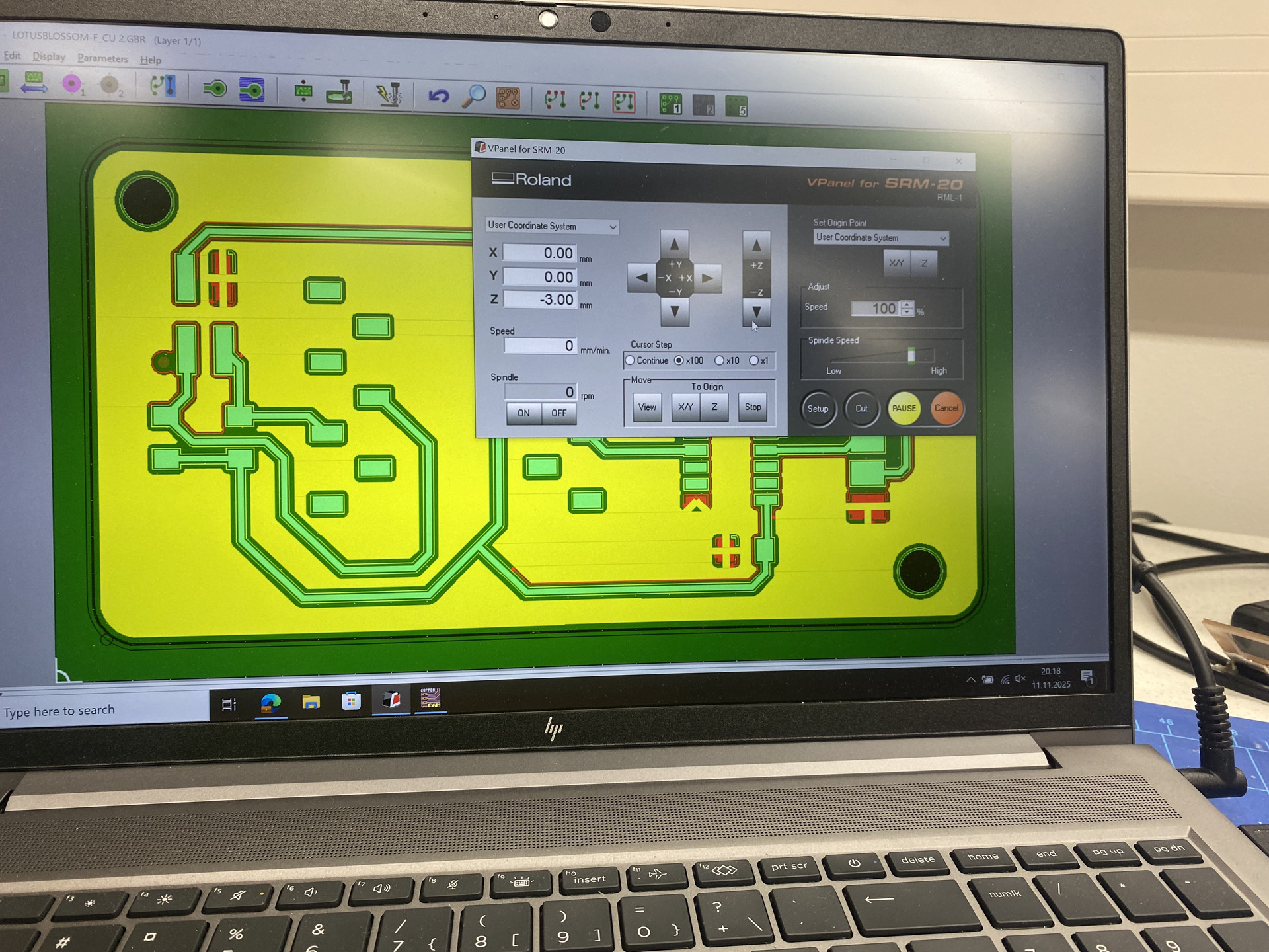
Then we set the origin, adjust the height (up the z by 3 mm), screw the machine drill that has 0.8 mm diameter but be sure to make it not too tight. Then from the computer we enter the drill.rml and edges.rml for the 0.8 mm drill. Then we repeat same process with a 0.2 mm diameter drill and the cu.rml and user1.rml files. Below is the control computer (The CopperCAM in the background ISN’T MINE! I only used the vPanel software):
Process video of milling:
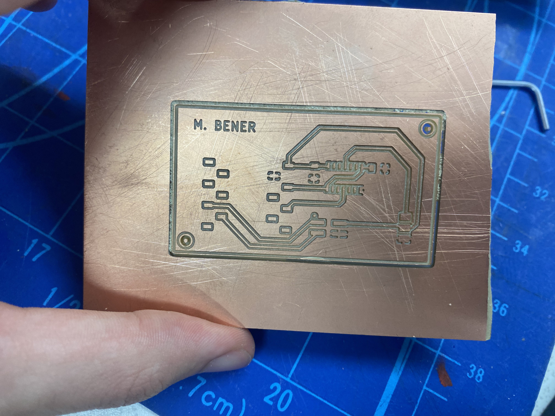
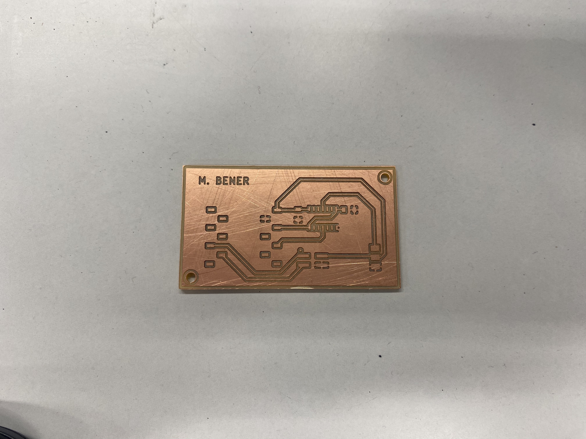
Below are some photos of the finished milled PCB:
Below is a process video of the testing of my board with a multimetre. The multimetre beeps when there is an electrical connection between the two points and doesn’t beep when there’s not.
My board passed all tests and all the electrical connections were stable.
Reflection
Thats it for today! We went from the lab to the hotel at about 10.30 PM. We were in the lab from 8 AM to 10.30 PM so about 14.5 hours including the lunch break .) It was tiring but tomorrow we start soldering, the real fun part :)